
View this article as a pdf
John Govier and Jim Rhodes of Inseto explain why sintering is required to get the best from silicon carbide’s electrical and thermal properties when used in EV power modules.
Electric and hybrid electric vehicles (EVs and HEVs) are creating a huge demand for power modules. They are also demanding lots from the modules, such as the ability to switch high voltages at high frequencies into loads that draw hundreds of Amps.
Deep power cycling is expected too. For example, thousands of maximum accelerations must be accommodated by channelling power from the battery pack to electric motors, as well as channelling energy back to the pack during regenerative braking.
Also (and as is the norm for the automotive sector), compact and lightweight form factors are required. So too is high reliability operation in harsh environments; in which temperature extremes and mechanical shocks and vibrations will be experienced.
Indeed, if you compare the requirements for consumer, industrial and automotive applications there are significant differences. Consumer electronics are designed to operate in a mild environment (0 to 40ºC temperature range and low humidity), a typical product life expectancy of two to five years is normal and failure rates of up 10% are considered acceptable. Industrial electronics must operate in a relatively harsh environment (-10 to 70ºC temperature range and higher humidity levels), a typical product life expectancy of five to 10 years is required, and failure rates should be well below 1%.
Automotive electronics is almost pushing into the realms of the military world. Systems, modules and components must (certainly for the powertrain), operate in an extremely harsh environment (-40 to 160ºC and 0 to 100% humidity), a life expectancy of up to 15 years is demanded and the goal is to have 0% failures. Also worthy of note is that many vehicle OEMs are now stipulating ‘zero reworks’, putting great pressure on the manufacturing and test processes of their suppliers.
High power
From a power perspective, silicon carbide (SiC) is today’s semiconductor material of choice for use in power modules, which typically contain several metal oxide semiconductor field effect transistors (MOSFETs) or insulated gate bipolar transistors (IGBTs) as the main power switching devices. For example, Tesla is recognised as one of the first mainstream vehicle manufacturers to embrace SiC-based power modules. Its Model 3 has a power inverter that includes 24 SiC-based power modules from STMicroelectronics. Each module has two SiC MOSFETs.
The increased use of SiC is part of the power semiconductor industry’s roadmap. For example, according to one integrated device manufacturer (IDM), in the early 1990s, a silicon (Si) IGBT fabricated on its 220µm process would have had a power density of circa 30kW/cm². As the IDM’s fabrication geometries shrank, device power density increased to about 70kW/cm² by the early 2000s. Most recently, switching from Si to SiC and to a 90µm process has enabled the IDM to achieve a power density of 250kW/cm².
Clearly, smaller and thinner dies mean a reduction in chip size and cost, higher efficiency (through lower losses) and an increase in power density. However, despite power losses being lower for SiC than for Si, these are relative to that higher power density.
Far more heat needs to be dissipated than before, and that is a challenge for device packaging.
The maximum operating temperature of a standard, plastic-encapsulated component (say in a TO 247-4 form factor) tends to be governed by its package. While some have a maximum operating temperature of 175ºC, this is far below the temperature at which MOSFETs and other switching structures fabricated using SiC have been proven to work. The maximum operating temperature is limited by properties of the plastic package and the adhesives or solders therein.
To benefit most from SiC’s ability to operate at a high temperature, it is best to attach bare die to a substrate that will provide good heat dissipation. Indeed, another advantage of SiC over Si is its high thermal conductivity, between 3 and 4W/(cm².K) compared to 1.5 4W/(cm².K).
The die must be metallised on the backside before it can be placed. This tends to be a tri-metal metallisation – adding a layer of titanium, then nickel, then silver (or sometimes gold). Bond wires, from the top of the die to module pins, have a role to play in heat dissipation. For standard high power electronic devices, aluminium wire or ribbon is used. The thermal conductivity of aluminium is about 2.3W/(cm².K). For SiC, copper (or copper clad in aluminium) is used. Its thermal conductivity is about 4W/(cm².K) and its electrical conductivity is better too.
A popular substrate is copper and for most applications, die can be soldered in place. Once again though, SiC pushes the envelope. The thermal conductivity of solder is not that good (circa 25W/(m.K) for lead-free solders, such as SnAg and SnAgCu) and its melting point is circa 220ºC.
The pressure’s on
An alternative to soldering is sintering. A paste comprising monometallic particles (of less than 1um in size) and a resin is printed, in the same way solder paste is applied to a PCB, onto a substrate in patterns corresponding to the shapes and locations of the SiC dies.
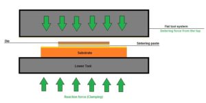
The substrate is heated to evaporate the resin and the dies are placed. The sintering process – which is often performed in an inert atmosphere (or on rare occasions a vacuum) to prevent the oxidisation of metal surfaces – is a combination of heat and pressure (a downwards force onto the tops of the dies).
The pressure, which can be up to a few tens of MPa, serves two purposes. Firstly, it means a lower temperature can be used to bond the materials, yet the bonds achieved will be able to operate at a higher temperature in the field. Secondly, it reduces the risks of voids, the presence of which are measured as a percentage of die area. Even a small void percentage can lead to delaminating and cracking over time, and a delaminated die can result in catastrophic failure because of the high currents being switched.
Silver is currently the most popular sintering material. Its melting point is about 960ºC and the thermal conductivity of a sinter paste is between 130 and 250W/(m.K). Figure shows 1 shows a SiC power semiconductor die silver-sintered to a silver-plated copper substrate.
Most sintering tools use a single, flat punch to apply force to the tops of the dies. However, die thickness will vary so the sinter material will not be compressed to the same extent for all dies. Multi-punch systems use multiple punches to apply force to groups of dies, but the problem still remains of accounting for different die thicknesses within each group. The solution, according to AMX Automatrix, is to have a single punch for each die; a solution the company has implemented in its patented micro-punch sinter tool (see figure 2).
While most sintering uses direct bonded copper (DBC) or ceramic substrates, research is being done into alternative substrates. According to a paper presented at the 11th International Conference on Integrated Power Electronics Systems (Berlin, Germany – March 2020) these alternatives include insulated metal substrates (IMS), copper lead-frames and high temperature stable PCBs.
As mentioned, and irrespective of the substrate onto which the dies are sintered, the contact between surfaces must be as near perfect as possible. There should be no voids. However, checking for voids requires the use of a scanning acoustic microscope (SAM) because x-ray equipment does not work – or rather the power required to penetrate the metallic substrate is so high it makes the die virtually invisible.
Summary
Sintering is undoubtedly the manufacturing process of choice for power modules that employ (and want to get the most from) SiC dies. The sinter must be as free of voids as possible if the module is to provide the performance and long-term reliability demanded by the EV and other sectors. Minimising the risk of voids beneath multiple small dies when sintered in a single process step requires multi-punch tools, and verification requires the use of SAM technology.
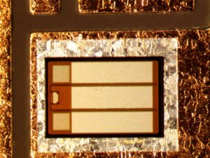
Figure 1: Above, a sintered SiC die. Image courtesy of AMX Automatrix.
 |
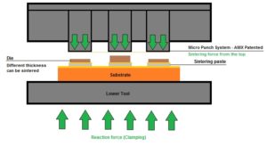 |
| Figure 2: Above, on the left, a standard flat, single punch sinter tool. Ideal if you are sintering a large, single die. Dies are getting smaller though and power modules are likely to have several dies with different thicknesses. The micro-punch system on the right applies equal force to all dies. Images courtesy of AMX Automatrix. | |
 |
 |
| Figure 3: On the left we have a SAM image of dies showing varying degrees of delamination. Deep power cycling (which equates to thermal cycling) will cause further delamination. On the right we have a SAM image of good sintering results. Images courtesy of AMX Automatrix.
|
|